How many patents does
Carl Zeiss Sms have?
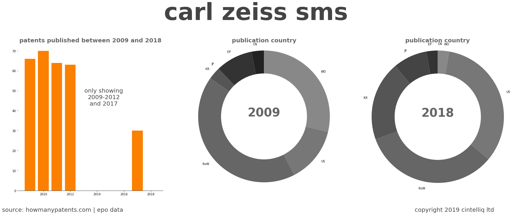
patents
572
families
132
granted
224
applications
348
US
192
WO
67
EP
51
KR
50
JP
37
CN
16
RoW
159
Buy the report
The report contains ten-year analysis with the following sections
- patent filing analysis
- worldwide filing analysis
- patent family analysis
- application analysis
- granted analysis
- classification analysis
- citation analysis
contact us for pricing
- VAT will apply to UK companies
- EU companies must supply their VAT number
Check out our sample pages |
Find companies to compare
Many companies now available
companies
12,000+
patents
42 million
patent families
23 million
Search to find companies of interest
read summary of their published patent
the following tables are just extracts from the report
the company report contains more information
Carl Zeiss Sms
Top ten assignees appearing on patents
2009 - 2018
| carl zeiss sms | 363 |
| carl zeiss smt | 98 |
| nawotec | 42 |
| carl zeiss | 19 |
| pixer technology | 12 |
| zeiss carl sms. | 6 |
| synopsys | 5 |
| carl zeiss nts | 5 |
| olympus corporation | 4 |
| carl zeiss meditec | 4 |
2009
| carl zeiss sms | 50 |
| nawotec | 10 |
| synopsys | 3 |
| pixer technology | 2 |
| olympus corporation | 1 |
| carl zeiss smt | 1 |
| carl zeiss | 1 |
| carl zeiss jena | 1 |
| carl zeiss nts | 1 |
| zeiss carl sms. | 1 |
2018
| carl zeiss smt | 20 |
| carl zeiss | 5 |
| carl zeiss sms | 4 |
| nawotec | 2 |
| carl zeiss meditec | 1 |
Carl Zeiss Sms
The top ten patent families are
|
Title of patent family (most common patent title) |
Family members |
Filing year |
|---|---|---|
| method for processing an object with miniaturized structures | 15 | 2008 |
| method and apparatus for analyzing and for removing a defect of an euv photomask | 14 | 2011 |
| method for electron beam induced etching | 13 | 2008 |
| methods and systems for removing a material from a sample | 13 | 2007 |
| method and apparatus for processing a substrate with a focussed particle beam | 12 | 2011 |
| method for electron beam induced etching of layers contaminated with gallium | 12 | 2008 |
| method and apparatus for correcting errors on a wafer processed by a photolithographic m… 🛈 | 11 | 2010 |
| method for electron beam induced deposition of conductive material | 11 | 2008 |
| method for determining a repair shape of a defect on or in the vicinity of an edge of a … 🛈 | 9 | 2008 |
| apparatus and method for investigating or modifying a surface with a beam of charged par… 🛈 | 9 | 2004 |